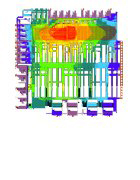
Increasing demand for smart electronic devices is driving integration and further miniaturization of integrated circuit (IC) technology. Interacting physics arising from shrinking geometries, especially in FinFETs, stacked-die and emerging 3D-IC architectures, result in power integrity and reliability-related design challenges. By simulating electromigration, thermal effects and electrostatic discharge phenomena, you can verify the power noise integrity and reliability of the most complex ICs. ANSYS simulation and modeling tools offer you early power budgeting analysis for high-impact design decisions and foundry-certified accuracy needed for IC sign-off.
At the core of every electronics system is a chip that has to meet multiple conflicting requirements, such as high performance, increased functionality, power efficiency, reliability and low cost. Ensuring the chip meets power integrity and reliability requirements as both a stand-alone component and within the electronics system calls for a system-aware chip design methodology. ANSYS uniquely offers a suite of multidomain, multiphysics solutions to support a chip-package-system (CPS) design flow.
With the cost of designing and implementing a system-on-chip (SoC) ranging from $50 million to $200 million, first-time working silicon is a must. IC designers require the most accurate simulation solution and consider foundry certification as the ultimate proof of accuracy. ANSYS semiconductor solutions have been certified at all leading foundries since 2006.
Our software has enabled thousands of successful tape-outs across multiple technology nodes. Our solutions are used by more than 90 percent of the global semiconductor companies, including all of the top 20.